PROCESS AND ENGINEERING SERVICES

As a vertically integrated manufacturer of opto-electronic components, APIC is ready to leverage its experience in design, wafer fabrication, packaging, and integration to offer best in class Process and Engineering Services to help you achieve your design goals. Contact APIC sales (sales@apichip.com) to see how we can help you achieve your design goals.

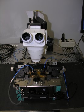
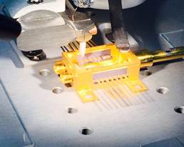
Laser Welding

With an alignment efficiency of greater than 95%APIC is able to laser weld in-package with our two-beam laser welder and omega-shaped clips.

We can work with fiber ferrules between 0.9 – 1.2 mm.
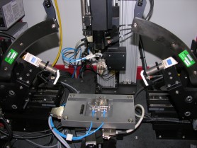
Die Attachment

APIC provides the ability to attach laser and photodetector dies from 0.3 x 0.3 mm to 2 x 2 mm in size to sub-mounts up to 40 mmin size.

Below are just some of the options that we can provide with this service:

Sub-mount materials

  1. AlN, Au coated
  2. AIN, solder coated
  3. CVD diamond, Au coated
  4. CVD diamond, solder coated

Choice of solders

  1. AuSn
  2. SnAg
  3. PbSn
  4. BiSn
  5. BiSnAg

Configuration of active devices

  1. P-side up
  2. P-side down

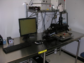
RF Testing

APIC provides top-notch testing for semiconductor lasers and photodiodes.

Device configuration options:

  1. on sub-mount
  2. in package


Tests we can run on lasers:

  1. LIV
  2. Spectra
  3. RIN


Tests we can run on photodiodes:

  1. Vf & VBr
  2. IDk
  3. Responsivity
  4. Saturation

Die Testing

APIC does die testing

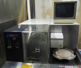
Wafer Dicing

APIC delivers the ability to cut wafers between 1 and 8 inches in diameter.

We can cut many materials, but the wafers we primarily cut are :

  1. Si
  2. AlN
  3. SiC

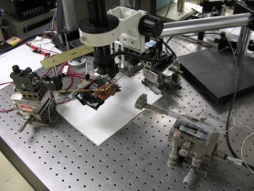
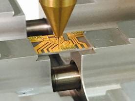
Wirebonding

APIC performs three main types of wirebonding:

  1. Ball
  2. Wedge
  3. Ribbon

We can perform wirebonding for devices that are either on a submount or in package.

Wirebonding Tests

APIC performs wire pull, ball shear, and die shear tests!
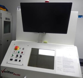
X-Ray Analysis

APIC performs failure analysis on voids of die attachment.