Location
Pasadena, CA
Job Description
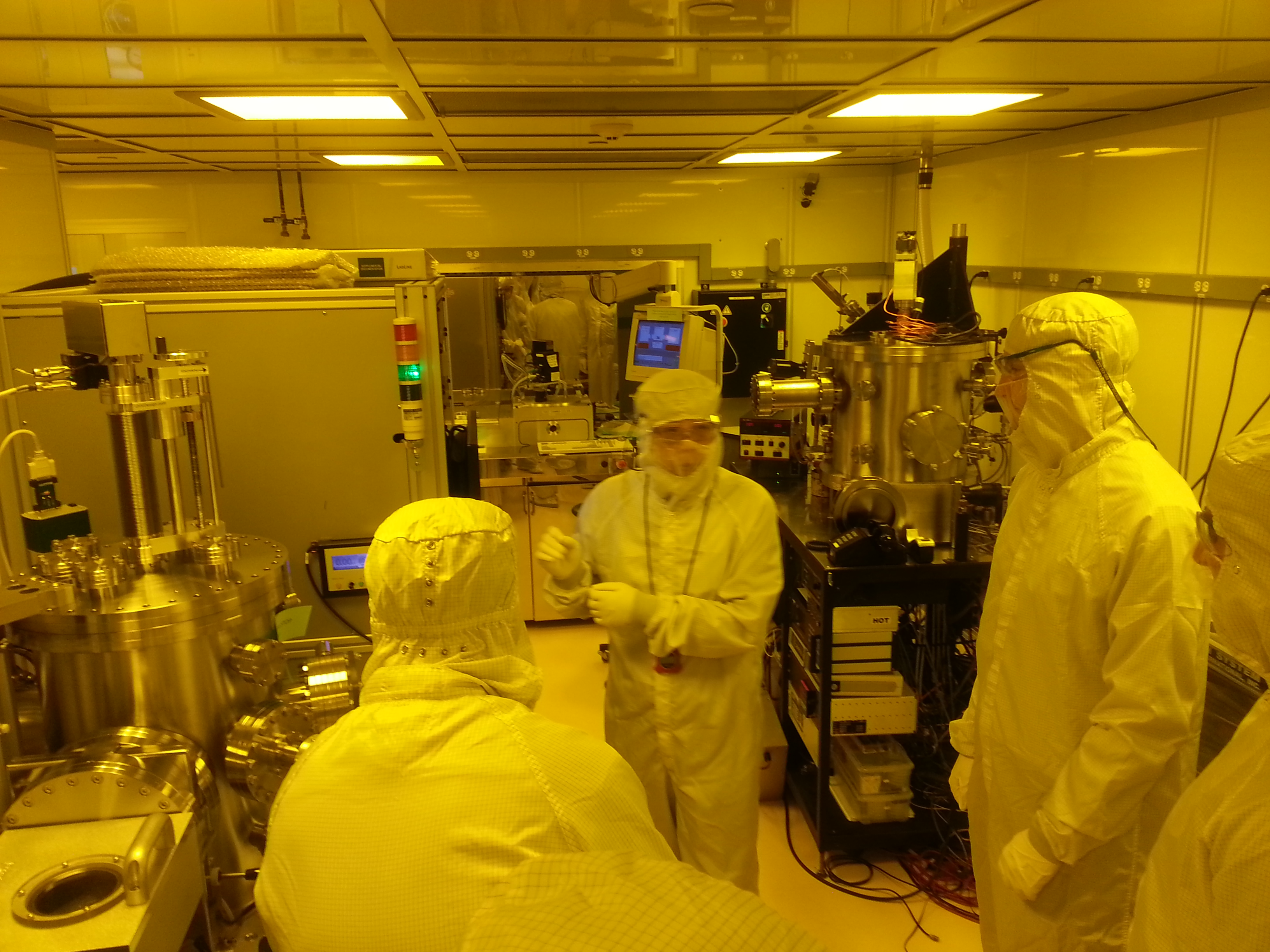
The processing engineer will work for APIC Corporation fabricating state of the art, high performance lasers and photodetectors and other photonic devices in Class 100 or better clean room facilities. Hours are flexible based on availability of required processing equipment. Some work may have to be performed in the evenings and/or on weekends, but 40 hours of work per week is expected/required.
Responsibility
The processing engineer is responsible for fabricating III-V semiconductor photonic devices including lasers and photodetectors in cleanroom environment according to established configuration controlled processes. The engineer will design and develop processes for new products using equipment including, but not limited to, photolithography, e-beam writing, wet etch, dry etch (RIE/ICP), dielectric film deposition (PECVD), metal deposition (CHA), sputter, electroplating, annealing, etc.
Requirements
- Minimum 3 years of industry experience in III-V semiconductor product development or production engineering.
- Minimum 5 years of hands-on experience in semiconductor processing and device characterization.
- Deep understanding of semiconductor physics and processes.
- Familiar with process equipment and clean room procedures.
- Can use inspection tools including SEM/FIB, etc.
- This position requires applicant to have U.S. Citizenship or Permanent Resident status.
Education and Experience
M.S. or PhD. in physics, applied physics, material science, electrical engineering, or related fields.
Application
Please email a copy of your resume to hr1@apichip.com